


No, IBM Is Not Becoming a Chipmaker — But It Just Revolutionized the Industry Anyway
No, IBM Is Not Becoming a Chipmaker — But It Just Revolutionized the Industry Anyway

Rich Duprey Thu, June 25, 2026 at 4:22 PM UTC
0
IBMQuick Read -
IBM's 0.7 nm Nanostack stacks transistors vertically, doubling chip density to 100 billion per chip with up to 50% more performance or 70% less power.
IBM licenses the Nanostack design to partners Samsung, Intel, and Rapidus, who are expected to commercialize the technology around 2030.
AI accelerators built on this architecture could deliver 7,000 TOPS, which is roughly seven times current hardware, reshaping data center economics as electricity costs soar.
Act now: the analyst who called NVIDIA in 2010 just named his top 10 AI stocks — and IBM didn't make the cut. Grab the names FREE today.
The semiconductor industry has spent the last decade racing toward a physical wall. Engineers have steadily shrunk transistors to pack more computing power onto ever-smaller chips, but that strategy is running out of room.
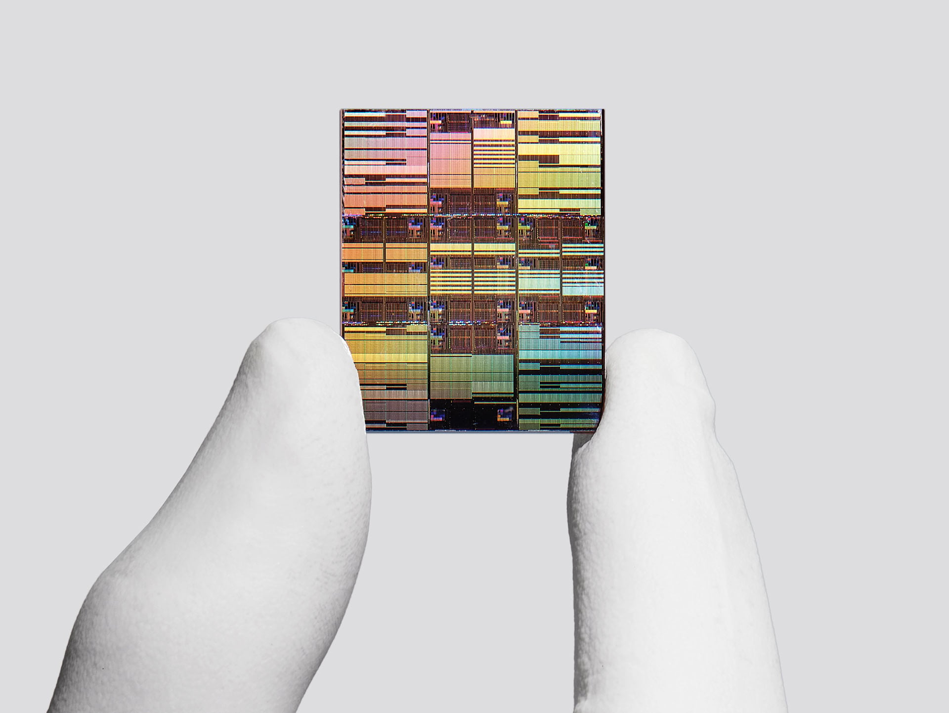
At today's leading-edge process nodes, components are measured in just a handful of atoms. Heat, power leakage, and manufacturing complexity have become major obstacles. That is why IBM's (NYSE:IBM) latest could revolutionize the industry. The company just unveiled a sub-1 nanometer chip design that could keep Moore's Law alive for years to come.
Yet despite the breakthrough, IBM is not getting back into the business of manufacturing chips.
IBM's Business Isn't Making Chips -- It's Inventing Them
Many investors hear "new chip" and immediately think of companies like Taiwan Semiconductor Manufacturing (NYSE:TSM), Intel (NASDAQ:INTC), or Nvidia (NASDAQ:NVDA). IBM occupies a very different role.
After selling its commercial semiconductor manufacturing business to GlobalFoundries in 2014, IBM transformed itself into one of the world's premier semiconductor research organizations. From its Albany, NY, research center, IBM develops next-generation chip architectures and licenses the underlying intellectual property to manufacturing partners.
That model allows IBM to avoid spending tens of billions of dollars building advanced fabrication plants while still influencing the direction of the industry.
The newly unveiled 0.7 nm "nanostack" design follows that playbook. IBM expects partners such as Samsung, Intel, and Japan's Rapidus to commercialize the technology over roughly the next five years.
Act now: the analyst who called NVIDIA in 2010 just named his top 10 AI stocks — and IBM didn't make the cut. Grab the names FREE today.
But to be clear, this is a research prototype, not a commercial product launch.
How IBM Broke Through Silicon's Limits
The most important detail is that "0.7 nm" is not a literal measurement of transistor size. Modern process nodes are largely marketing labels that represent advances in chip architecture and density.
Historically, chipmakers improved performance by shrinking transistors horizontally across a flat silicon surface. That approach has largely reached its practical limits because components are already only a few atoms wide. IBM's answer is what it calls 3D Sequential Integration, or Nanostack.
Instead of placing transistors side by side, IBM stacks them vertically. The result is a fingernail-sized chip capable of housing approximately 100 billion transistors -- roughly double the density of today's leading 2 nm designs.
Advertisement
Here's how IBM could change the game:
Metric
Current Leading-Edge Chips
IBM 0.7 nm Nanostack
Transistor Density
~50 billion
~100 billion
AI Processing Power
Baseline
Up to 7,000 TOPS
Performance Gain
Baseline
Up to 50% higher
Power Consumption
Baseline
Up to 70% lower
Source: IBM Research announcement and technical briefing.
Why Investors Should Pay Attention
This breakthrough matters because it extends the computing roadmap for artificial intelligence.
Training frontier AI models currently requires months of processing time and enormous energy consumption. IBM estimates a specialized AI accelerator built on its 0.7 nm architecture could deliver up to 7,000 trillion operations per second, or TOPS, roughly seven times current AI hardware capabilities.
The architecture also improves SRAM scaling by 40%, allowing processors to keep more data close to the computing cores. That reduces bottlenecks and speeds up AI inference tasks such as text generation, image creation, and reasoning.
Data centers may be the biggest beneficiaries. Operators could choose between:
Up to 50% more performance at existing power levels.
Up to 70% lower power consumption while maintaining current performance.
That flexibility could reshape data center economics as electricity becomes one of AI's largest operating expenses.
Granted, commercialization remains years away. Manufacturing sub-1 nm chips will require the industry's most advanced High-NA EUV lithography systems from ASML (NASDAQ:ASML), machinery that costs hundreds of millions of dollars per unit. That reality likely strengthens the competitive positions of Taiwan Semiconductor, Samsung, Intel, and government-backed ventures like Rapidus.
Key Takeaway
In short, IBM's announcement is not the return of a commercial chipmaker. It is the latest example of IBM doing what it has done for decades -- inventing the future and letting others manufacture it.
The significance isn't that IBM built a 0.7 nm prototype. It's that the company demonstrated a path around the physical limits that threatened to slow artificial intelligence, cloud computing, and high-performance computing.
If IBM's manufacturing partners can bring this technology to market around 2030, investors may look back on this announcement as the moment the semiconductor industry's next decade of growth was secured.
Act now: the analyst who called NVIDIA in 2010 just named his top 10 AI stocks — and IBM didn't make the cut. Grab the names FREE today.
Source: “AOL Money”
